PCBA solution design service is very suitable for small and medium-sized enterprises or individuals without self-established design teams. Fartai electronics converts customers' design concepts into concrete and feasible technical solutions, providing one-stop overall manufacturing solutions from functional requirements discussion to hardware and software design and product manufacturing. Fartai electronics has been focusing on the design of PCBA solutions for over 20 years. It has an independent design team in design, development, DFM analysis, proofing and mass production. The team leader has more than 20 years of PCBA board processing experience. At the same time, according to different customer needs, to provide a responsive flexible way of cooperation. In order to seize the consumer market and transform product concepts into physical products, an experienced and technical support PCBA solutions company is required to collaborate. We are your first choice!
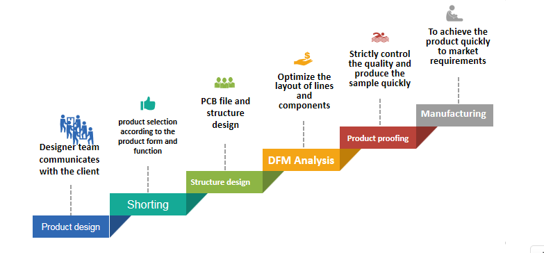
Schema Development —— PCBA solution design process
Product Design
The designer team will communicate with the customer to describe the product design ideas, functional requirements and appearance requirements. We will respond quickly and provide the design plan and documents within 48 hours.
Sorting
According to the product form and function of the design scheme, select the product materials, and select the electronic components required by the product, such as IC, capacitor and battery, CPU, Sensor, etc., which determine the battery life of the product.
Structure design
PCB documentation and structural design, generate PCB boilerplate, ensure its reliability, functionality, stability and feasibility. Allows structural validation of designs against product requirements, greatly reducing risk.
DFM Analysis
The engineer analyzed PCB proofing documents, further optimized the layout of circuits and components, performed DFM analysis, identified the defects of PCBA design scheme, improved and improved PCBA manufacturing yield, and reduced the cost of after-sales service.
Product proofing
PCBA sample is the design concept of realizing the product. After the design plan of PCBA is quickly determined by the engineer team, the time of technical preparation, component procurement, process control, test and other links is shortened to strictly control the quality and make the sample quickly.
Manufacturing
From design to mass production process, we strive to shorten the product development cycle, optimize the design, to achieve mass production. Fartai electronics has 2 fully automatic SMT production lines and 2 DIP plug-in lines to achieve mass production standardization, automation and improve production efficiency. To achieve the product quickly to market requirements.
Schema Development —— PCBA solution design process