Processing of high precision Multilayer PCB
Processing of high precision Multilayer PCB
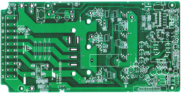
With the development of modern electronic technology and the high-speed and integration of chips, the electromagnetic environment inside and outside various electronic equipment systems is more chaotic, so the multi-layer PCB processing is particularly important. Compared with single panel, double panel requires higher technology and processing skills. It is multi-layer lamination, high-quality multi-layer PCB processing. Multilayer PCB, precision Multilayer PCB production, Shenzhen wanchuangxing Electronics Co., Ltd. A complete set of imported automatic production line, with various surface treatment equipment. In fact, the overall price of multi-layer board must also be based on the basis of multi-layer board proofing. Only when the samples are qualified, the products can be produced in batches; if the product size is relatively large, it can be satisfied. In the whole process of multi-layer board proofing, it is necessary to ensure that each revision meets the conditions and requirements, otherwise the inventory can only be disposed as scrap, which is really a very painful understanding.
1. Impedance characteristics of printed circuit board
According to the theory of signal transmission, the signal is a function of time and distance variables, so every part of the signal on the line may change. Therefore, it is confirmed that the ratio of the change of voltage to the change of current is the characteristic impedance of the transmission line: the characteristic impedance of the transmission line is only related to the characteristics of the signal line itself. In practical circuits, the resistance value of the conductor itself is less than the system's dispersion impedance, especially in high frequency circuits, the characteristic impedance mainly depends on the unit dispersion capacitance of the wire and the dispersion impedance brought by the unit dispersion inductance. The characteristic impedance of the ideal transmission line only depends on the unit dispersion capacitance and the unit dispersion inductance of the line.
2. Calculation of characteristic impedance of printed circuit board
The proportional relationship between the rising edge time of the signal and the time needed for the signal to be transmitted to the receiving end determines whether the signal line is regarded as the transmission line. The detailed proportion relationship can be explained by the following formula: if the wire length on the PCB is longer than L / B, the connecting wires between signals can be regarded as transmission lines. From the calculation formula of signal equivalent impedance, we can see that the impedance of transmission line can be expressed by the following formula: in the case of high frequency (tens of MHz to hundreds of MHz), it is satisfied with WL > > R (of course, in the range of signal frequency greater than 109hz, considering the skin effect of signal, we need to study this relationship carefully). For the confirmed transmission line, the characteristic impedance is a constant. The reflection phenomenon of signal is caused by the inconsistency of characteristic impedance between the driving end of signal and transmission line, as well as the impedance of receiving end. For CMOS circuits, the output impedance of the driving end of the signal is relatively small, which is tens of ohms. The input impedance of the receiver is relatively large.
3. PCB characteristic impedance control
The characteristic impedance of conductor on PCB is an important index of circuit planning, especially in the PCB planning of high frequency circuit, it is necessary to consider whether the characteristic impedance of conductor is consistent with that required by device or signal, and whether it matches. Therefore, it is necessary to pay attention to two concepts in PCB reliability planning.
4. PCB impedance control
There are all kinds of signal transmission in the conductor of the circuit board. When it is necessary to improve its transmission rate and frequency, if the circuit itself is different due to etching, lamination thickness, wire width and other factors, it will form impedance value change, resulting in signal distortion. Therefore, the impedance value of the conductor on the high-speed circuit board should be controlled within a certain range, which is called "impedance control". The main factors that affect the impedance of PCB wiring are the width of copper wire, the thickness of copper wire, the dielectric constant of medium, the thickness of medium, the thickness of pad, the way of ground wire, the wiring around the wiring, etc. Therefore, when planning PCB, it is necessary to control the impedance of the wiring on the board, so as to avoid signal reflection and other electromagnetic interference and signal integrity problems as far as possible, and ensure the stability of the actual use of PCB. The calculation method of microstrip and stripline impedance on PCB can refer to the corresponding empirical formula.
Jiangmen printed circuit board http://www.fartai.com/